Example 1.6
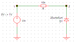
Schematic
HSPICE Netlist
* Example 1.6
* diode model
.MODEL D D CJO=0.2fF PB=0.9
**CJO:capacitance at 0V bias
**PB:Built-in diode contact potential
* main circuit
R 1 2 10k
D1 0 2 D 100
* input voltage signal
Vin 1 0 Pulse(0 1 100f 100f 100f 2.5n 5n)
* analysis
.op
.tran 0.01n 10n
* options
.options post
.end
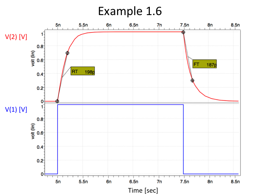
Simulation Result
rise time = 0.20ns
fall time = 0.19ns


I believe that the intended zero-bias depletion capacitance in the netlist provided for ex1.6 should be CJO=20f, not CJO=0.2f, as the diode has an area of 20um x 5um = 100um^2. Multiplying the capacitance/area is 0.2fF/um^2 x 100um^2 = 20fF.
I believe the netlist is correct. The model parameter CJO is the specific capacitance, per unit area, following the same notation as in the book. When the diode D1 is instantiated, its’ area is specified by the last number: 100. Hence, the zero-bias capacitance of the diode is the model parameter CJO times the area 100, giving 20fF as you said.