0.8um CMOS process
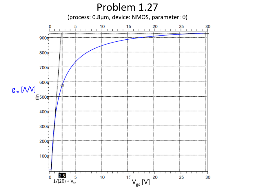
1. unCox, Vtn, θ for NMOS
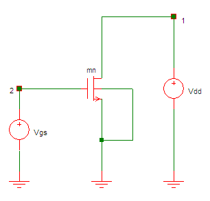
1-1. Schematic
1-2. HSPICE Netlist
* Problem 1.27 uCox, Vtn for 0.8um NMOS
* MOS model
.include p8_cmos_models.inc
* main circuit
mn 1 2 0 0 nmos L=1.6u W=16u
* power supply
vdd 1 0 5
*vdd 1 0 40 ***for theta
vgs 2 0 1
* analysis
.op
.dc Vgs 0 1 1m
*.dc Vgs 0 30 1m ***for theta
* options
.options post
.end
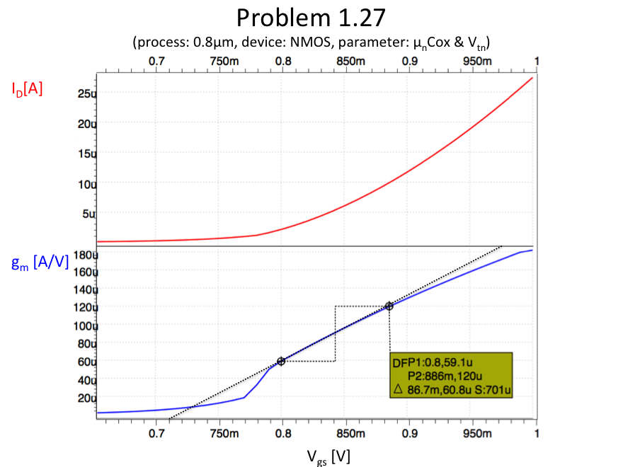
1-3. Simulation Result
2. Lambda for NMOS
2-1. Schematic
2-2. HSPICE Netlist
* Problem 1.27 lambda for 0.8um NMOS
* MOS model
.include p8_cmos_models.inc
* main circuit
mn 1 2 0 0 nmos L=1.6u W=16u
* power supply
vdd 1 0 5
vgs 2 0 1
* analysis
.op
.dc Vdd 0 1 10m
* options
.options post
.end
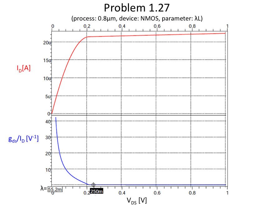
2-3. Simulation Result
λ = 0.0552 V-1 @ L = 1.6 μm
λL = 0.088 μm/V
3. Cov/W for NMOS
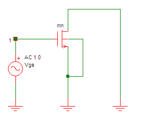
3-1. Schematic
3-2. HSPICE Netlist
* Problem 1.27 Cov/W for 0.8um NMOS
* MOS model
.include p8_cmos_models.inc
* main circuit
mn 0 1 0 0 nmos L=1.6u W=16u
* power supply
vgs 1 0 dc=0 ac=1
* analysis
.op
.ac dec 100 1 1k
* options
.options post
.end
3-3. Simulation Result
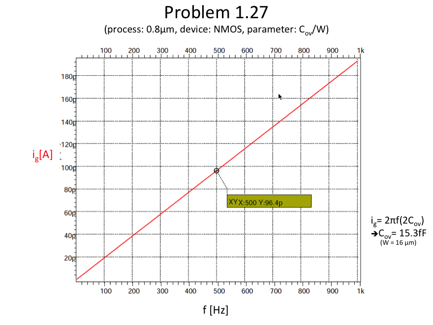
Cov = 15.3 fF @ W = 16 μm
Cov/W = 0.96 fF/μm
4. Cdb/W for NMOS
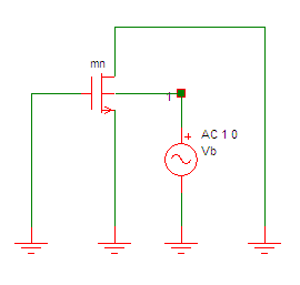
4-1. Schematic
4-2. HSPICE Netlist
* Problem 1.27 Cdb/W for 0.8um NMOS
* MOS model
.include p8_cmos_models.inc
* main circuit
mn 0 0 0 1 nmos L=1.6u W=16u
* power supply
vb 1 0 dc=0 ac=1
* analysis
.op
.ac dec 100 1 1k
* options
.options post
.end
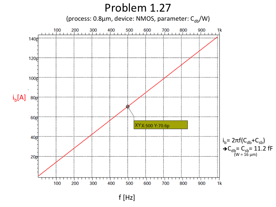
4-3. Simulation Result
Cdb = 11.2 fF @ W = 16 μm
Cdb/W = 0.70 fF/μm
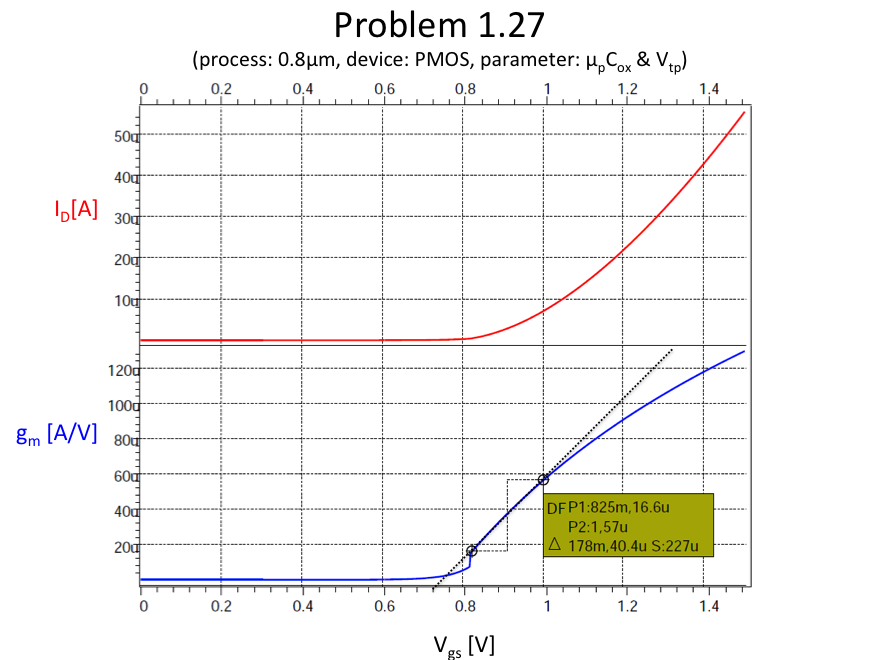
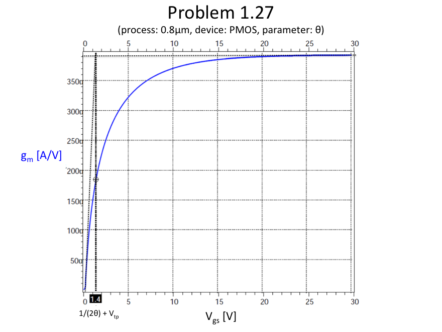
5. upCox, Vtp, θ for PMOS
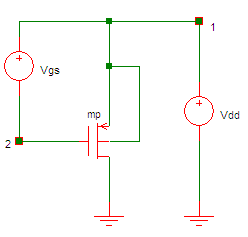
5-1. Schematic
5-2. HSPICE Netlist
* Problem 1.27 uCox, Vtp for 0.8um PMOS
* MOS model
.include p8_cmos_models.inc
* main circuit
mp 0 3 2 2 pmos L=1.6u W=16u
* power supply
vdd 1 0 5
*vdd 1 0 40 ***for theta vgs 1 2 1
* analysis
.op
.dc vgs 0 1.5 1m0
*.dc vgs 0 30 1m0 ***for theta
.print i(v0)
* options
.options post
.end
5-3. Simulation Result
6. lambda for PMOS
6-1. Schematic
6-2. HSPICE Netlist
* Problem 1.27 lambda for PMOS
* MOS model
.include p8_cmos_models.inc
* main circuit
mp 0 3 2 2 pmos L=1.6u W=8u
* power supply
vdd 1 0 5
vgs 2 3 1.2
v0 1 2 dc 0
* analysis
.op
.dc vdd 0 5 1m0
.print i(v0)
* options
.options post
.end
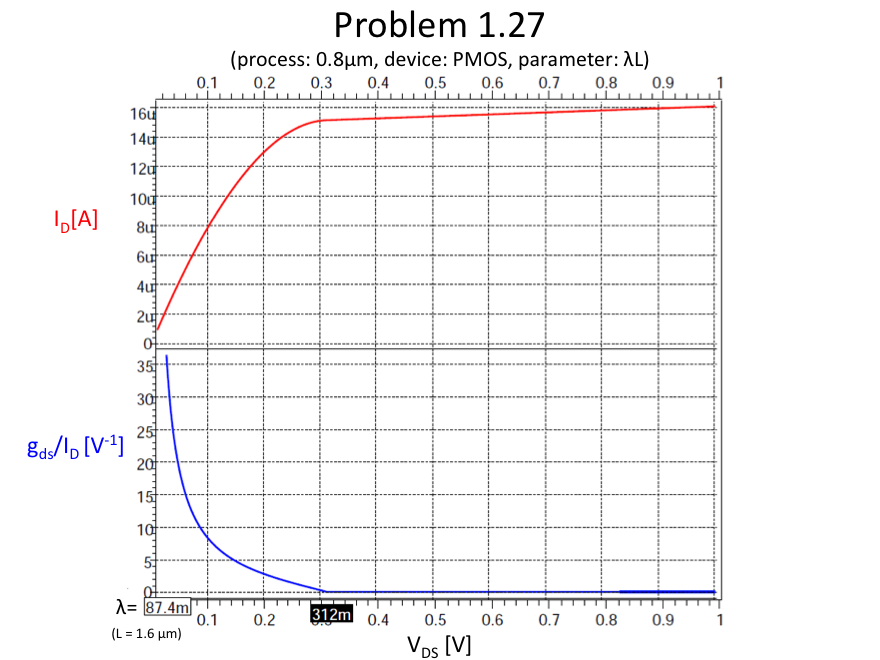
6-3. Simulation Result
λ = 0.088 V-1 @ L = 1.6 μm
λL = 0.14 μm/V
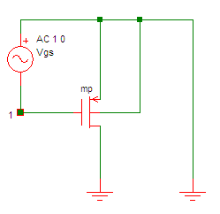
7. Cov/W for PMOS
7-1. Schematic
7-2. HSPICE Netlist
* Problem 1.27 Cov/W for 0.8um PMOS
* MOS model
.include p8_cmos_models.inc
* main circuit
mp 0 1 0 0 pmos L=1.6u W=16u
* power supply
vgs 1 0 dc=0 ac=1
* analysis
.op
.ac dec 100 1 1k
* options
.options post
.end
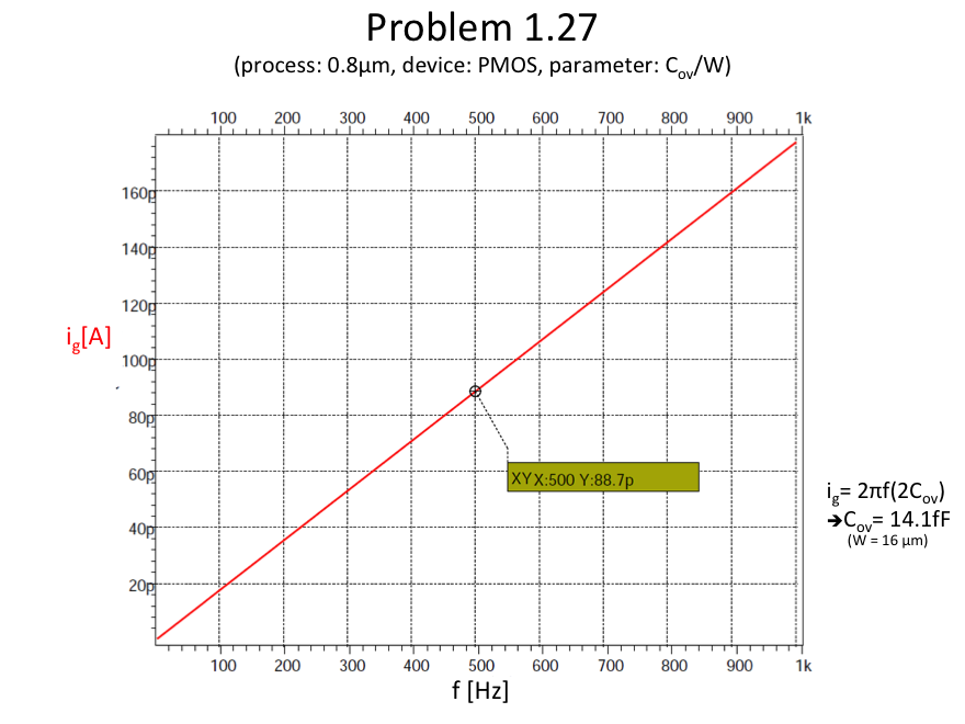
7-3. Simulation Result
Cov = 14.1 fF @ W = 16 μm
Cov/W = 0.88 fF/μm
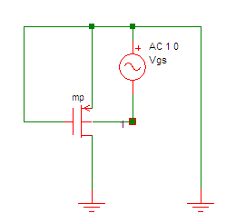
8. Cdb/W for PMOS
8-1. Schematic
8-2. HSPICE Netlist
* Problem 1.27 Cdb/W for 0.8um PMOS
* MOS model
.include p8_cmos_models.inc
* main circuit
mp 0 0 0 1 pmos L=1.6u W=16u
* power supply
vb 1 0 dc=0 ac=1
* analysis
.op
.ac dec 100 1 1k
* options
.options post
.end
Interesting post, I’ll pobabrly look into this more if I get a chance. How would you combat WPE? Is making the transistor length and/or width larger to minimize the effects of WPE the only option, or are there process steps that can be modified as well? From what little I know about the process side of things it seems taking this route would be more expensive and could hurt yield.As for my work being affected by scaling, being a student means I have to learn about all sorts of short channel effects which makes me marvel at how we can even get transistors to still work anymore there’s so many trade offs. When you look at the long channel model and see how it starts to fail even at ~1um lengths, the true scale of designing devices comes into focus.